
Join Us
Join Us
1. Social insurance and housing fund.
2. Annual health check and supplementary medical insurance, annual leave and additional paid leave.
4. Team building, welfare, birthday celebration.
5. Performance awards and stock options.
6. Training and promotion opportunities.
7. Free staff dormitory (Wuxi)
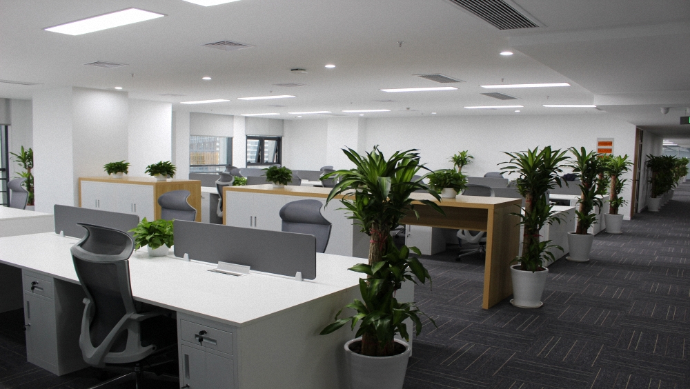
8. Gym and recreation area (Wuxi and Shanghai office)
9.Complimentary breakfast, afternoon tea, fruit of the day
Please submit your resume to our HR, email: hr@unimcom.com
Work City
ShangHai
Work City
ShangHai
Job Responsibilities:
1. Responsible for chip analog circuit design and simulation
400-990-2897
Monday to Friday 08:30-17:30
![]()

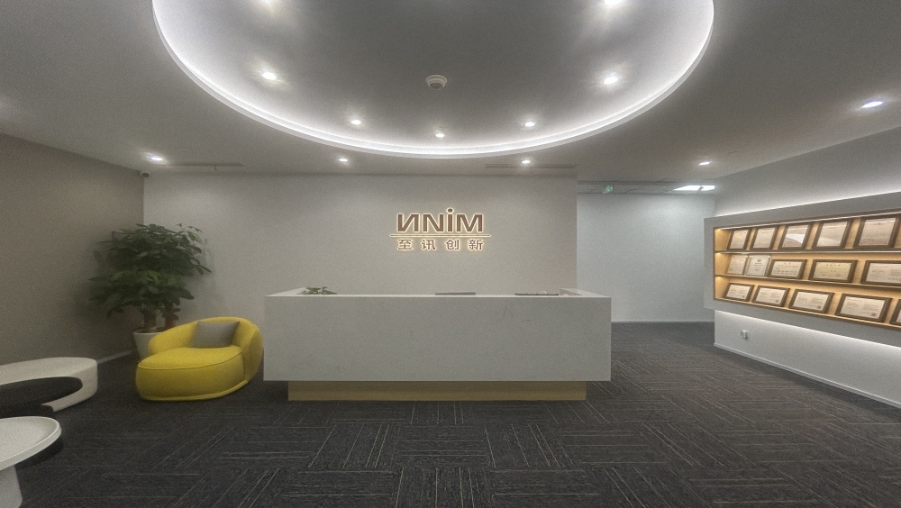
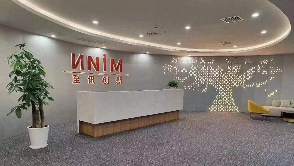
UNIM Innovation
UNIM Semi